本篇文章參考
ACPI Specification Version 6.3
Vol. 1: Intel® 200 and Z370 Series Chipset Families PCH
Vol. 2: Intel® 200 and Z370 Series Chipset Families PCH
Fixed ACPI Description Table (FADT)
| Field | Byte Length | Byte Offset | Description |
| Signature | 4 | 0 | 'FACP' |
| ...... | ...... | ...... | ...... |
| GPE0_BLK | 4 | 80 |
GPE 0 Register Block 的 port address。 若不support,則值為0。 |
| GPE1_BLK | 4 | 84 |
GPE 1 Register Block 的 port address。 若不support,則值為0。 |
| ...... | ...... | ...... | ...... |
| GPE0_BLK_LEN | 1 | 92 |
GPE 0 Register Block 所decode 的bytes 長度。 其值必為2的正指數冪。 |
| GPE1_BLK_LEN | 1 | 93 |
GPE 1 Register Block 所decode 的bytes 長度。 其值必為2的正指數冪。 |
| GPE1_BASE | 1 | 94 |
GPE1 events在ACPI general-purpose event中 的offset。GPE0 events 的offset為0。 |
| ...... | ...... | ...... | ...... |
General-Purpose Event Register Blocks
ACPI spec在 FADT table定義了兩組 GPE register blocks:GPE 0與 GPE 1。register block包含 enable 與 status register (ex:GPE0_EN與 GPE0_STS),這兩個 register長度各佔 register block長度的 一半,所以 FADT中 register block的長度 GPE0_BLK_LEN與 GPE1_BLK_LEN必為 2的冪次。
使用RWEverything讀取GPE Register Block
從 FADT table 中可得 GPE0的 IO port addresss為 0x1880,和其使用的長度為 0x20。
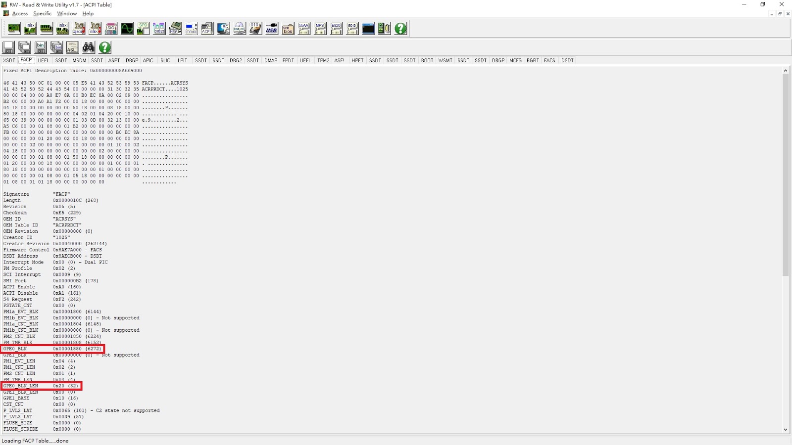
與 Intel PCH spec對照,可從 PMC Controller (D31:F2)的 Offset 40-43h讀出 ACPI Base Address,用 RW讀出其值為 0x1801,bit 1代表為 IO space,所以其 IO address為 0x1800。


與 Spec中的 PMC I/O Based Register 對照,Offset 0x80為 GPE0 block register起始位置,跟 FADT table位置為0x1880 (0x1800 + 0x80) 符合。

再用RW 讀取IO address 0x1880,就可得出GPE0 Register Block位置。若要知道GPE register 每 個bit實際上對應的 GPIO pin,則需參考chipset的相關設定。

GPIO
配置 GPIO用以產生 SCI event
要將 GPIO配置成 GPE的 source,要先將 GPIO配置成可以產生 SCI。需先將 GPI General Purpose Event Enable設起來。

還要配置 Pad Configuration中的 GPIROUTSCI bit。

\_GPE
為ACPI predefined 的namespace,用以處理GPE register block中的General events。
使用RWEverything讀取\_GPE
以我所使用的主機板為例,\_GPE中定義了_E02 的Method,表示其為 handle GPE0_STS bit2 edge event的method。

沒有留言:
張貼留言